

| Test Type | Inspection Object | Black-and-White Imaging | Pseudocolor Imaging | Imaging Analysis |
|---|---|---|---|---|
| PL testing | Crystalline Silicon Solar Cell |  |  | The crystalline quality and carrier lifetime are evaluated by means of PL signal intensity distribution: bright areas correspond to regions with intact crystallization and long carrier lifetimes, while dark lines/dark spots indicate defects such as microcracks, metallic impurities or oxygen-carbon precipitates, allowing the quantitative measurement of defect distribution density and affected range. |
| Perovskite Solar Cell |  |  | Analysis of Thin Film Uniformity and Defect State Density: The uniformity of luminescence intensity reflects the consistency of thin film preparation; dark spots correspond to defect-enriched regions or interfacial recombination centers, and component segregation can be determined by means of peak position characteristics. | |
| Perovskite Tandem Solar Cell - Perovskite Layer | 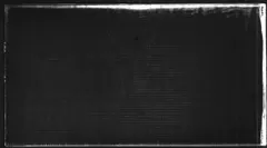 | 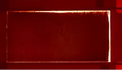 | Focusing on the Intrinsic Properties and Interface Matching of the Perovskite Layer: Evaluate the thin film crystallization quality and the degree of interfacial recombination with the transport layer. Abnormal luminescence decay regions indicate excessively high interface state density, which impairs the carrier separation efficiency. | |
| Perovskite Tandem Solar Cell - Crystalline Silicon Layer | 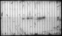 |  | Targeted Detection of Defects and Carrier Transport in the Crystalline Silicon Layer: Excluding interference from the perovskite layer, it identifies defects such as microcracks and impurity contamination in the crystalline silicon layer, quantifies carrier lifetime via signal intensity, and determines the impact of the tandem structure on the performance of the crystalline silicon layer. | |
| EL testing | Crystalline Silicon Solar Cell |  | 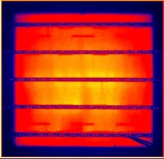 | EL enables the identification of electrode contact abnormalities and the evaluation of carrier transport performance: via EL imaging, it can assist in judging the status of carrier transport; combined with EL imaging, it can identify electrode contact anomalies, and dark areas can also indicate structural defects such as microcracks and grid breaks. |
| Perovskite Solar Cell | 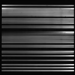 | 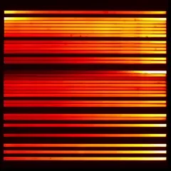 | Identification of Defect Types and Current Distribution Uniformity: Dark spots correspond to laser scribing deviations, microcracks or material defects; uneven grayscale indicates abnormal current distribution caused by differences in thin film thickness or composition, enabling the tracing of process issues such as lamination and encapsulation. | |
| Perovskite Tandem Solar Cell - Perovskite Layer | 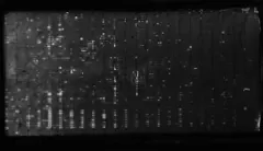 | 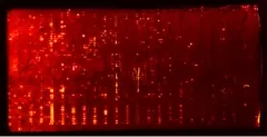 | Evaluation of Interlayer Compatibility and Current Matching: The contact quality between the perovskite layer and the intermediate connecting layer is detected; abnormal luminescence regions reflect carrier injection/extraction barriers, providing a basis for optimizing the tandem interface structure. | |
| Perovskite Tandem Solar Cell - Crystalline Silicon Layer | 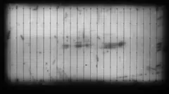 | 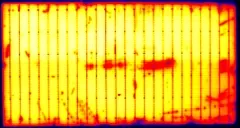 | Evaluation of Interlayer Compatibility and Current Matching: Detect the contact quality between the perovskite layer and the intermediate connecting layer; abnormal luminescence regions reflect carrier injection/extraction barriers, providing a basis for optimizing the tandem interface structure. Analysis of Electrode Performance and Overall Synergy of the Crystalline Silicon Layer: Focus on identifying contact defects between the crystalline silicon layer and the tandem electrode; judge the matching degree of carrier transport between the two layers by means of luminescence intensity distribution, so as to avoid efficiency attenuation caused by local current congestion. |
For the detailed performance parameters of this device, please refer to the relevant section:Crystalline Silicon/Perovskite PL/EL Integrated Tester
contact
Be the first to know about our new product launches, latest blog posts and more. Nanjing Vision Potential Intelligent Technology Co.,Ltd.Established based on the Nanjing Xiangning Artificial Intelligence Research Institute, we have brought together a number of outstanding industry... Any question or request?
Click below, we’ll be happy to assist. contact