
In the manufacturing process of solar cells, the inspection stage is crucial. Although the traditional Electroluminescence (EL) inspection method is effective, it has limitations in certain scenarios. To further improve inspection efficiency and accuracy, Photoluminescence (PL) inspection technology has emerged. Next, we will delve into the application of PL inspection technology in the solar cell manufacturing process.
As photovoltaic wafers develop toward larger sizes and thinner thicknesses, solar cells are more prone to chipping and microcracks during production. However, the traditional EL inspection method is contact-based, which may further cause microcracks or chipping during the inspection process.
In the key process steps of solar cell production, such as diffusion, etching, annealing and anti-reflective coating deposition, various defects may occur, including microcracks, ghosting marks, black spots, conveyor belt imprints and abnormal diffusion. These defects are often difficult to monitor in real time during the manufacturing process, and most of them are caused by improper operator operations or abnormal process parameters.
At present, most solar cells undergo final inspection using EL equipment after being manufactured into finished products, and then potential problems in the manufacturing process are traced retroactively. This method has significant lag and leads to unnecessary waste of materials and labor.
PL inspection determines whether solar cells have defects by exciting fluorescence with lasers. Its working principle is to use lasers of specific wavelengths to excite electrons in solar cells, causing the electrons to transition from the ground state to the excited state and emit infrared fluorescence. The fluorescence intensity is proportional to the concentration of non-equilibrium minority carriers in the solar cells, so it can be used to judge whether the cells have defects, impurities and other issues that affect cell efficiency.
Compared with EL inspection, PL inspection has the following advantages:
Non-contact inspection: Avoids further damage to solar cells during testing
High-sensitivity and high-resolution imaging: Enables more accurate detection of micro-defects on solar cells
Real-time process monitoring: Improves production efficiency and product quality
The PL inspection solution for solar cells is designed to detect internal defects of cells, such as microcracks, black spots, scratches and indentations, thereby ensuring the accuracy and reliability of inspection results. In addition, the solution also involves the determination of module parameters, including object distance, angle and structure.
Due to the varying excitation efficiency of solar cells to specific laser wavelengths at different process stages, the inspection effects of cells at each stage differ, and the corresponding parameter settings need to be adjusted accordingly. In addition, the excitation efficiency of different regions of silicon wafers processed through certain specific process stages will also change. For detailed inspection effects of solar cells at each process stage, please refer to the following content:
In the entire production process of solar cells, after refined processing through various stages, the finished cells finally enter the inspection stage. The imaging effects of cells at the Plasma Enhanced Chemical Vapor Deposition (PECVD) stage and post-coating stage are particularly excellent.
After confirming the excellent PL imaging effects of cells at the PECVD stage, finished cell stage and post-coating stage, we will further elaborate on the specific implementation methods of inspection and installation. The core of the solution lies in the accurate inspection of imaging effects at key stages such as PECVD and finished cells. The equipment installation process must ensure the inspection accuracy and operational stability of each process stage.
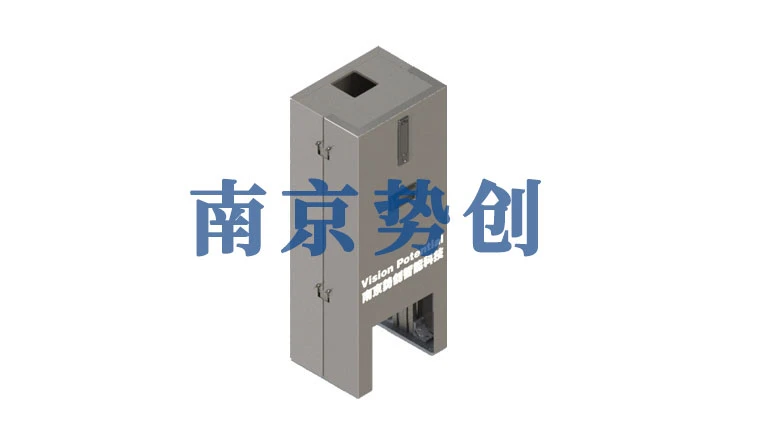
The SC-PL Series Integrated Machine Vision Imaging Module integrates high precision and fast response performance, and is suitable for various complex production environments to meet inspection requirements in different scenarios. As an innovative product independently developed by Nanjing Shichuang Intelligence, this module can continuously output high-quality visual images in various application scenarios and ensure long-term stable operation of equipment.
Integrating multiple functions including camera, laser, protection, synchronization and control, the module has become an industry-leading choice with its high precision, fast inspection speed, convenient deployment, simple operation and excellent stability. Adopting top-tier imported imaging devices, the SC-PL Series maintains outstanding stability even under high-speed movement of 60-100 km/h and high-precision operation of 0.1-0.5 mm.
The Raw Silicon Wafer PL Inspection Module developed by Vision Potential is a professional device for silicon wafer quality inspection based on the photoluminescence principle of silicon materials. The device utilizes the intrinsic excitation luminescence characteristics of silicon: when silicon atoms are excited, electrons transition from the valence band to the conduction band, and then emit fluorescence when transitioning back from the conduction band to the valence band. The PL intensity is negatively correlated with defect density and recombination center concentration, so the quality of silicon wafers can be evaluated by detecting PL signals. The raw silicon wafer PL inspection technology can be widely applied in the early production stages of photovoltaic products such as silicon ingots, raw silicon wafers and textured wafers. It can conduct quality inspection in the early process steps before and after cell diffusion, achieving the dual goals of product quality control and manufacturing cost reduction.
contact
Be the first to know about our new product launches, latest blog posts and more. Nanjing Vision Potential Intelligent Technology Co.,Ltd.Established based on the Nanjing Xiangning Artificial Intelligence Research Institute, we have brought together a number of outstanding industry... Any question or request?
Click below, we’ll be happy to assist. contact